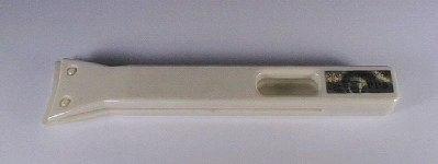
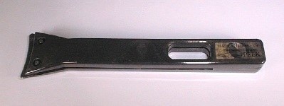
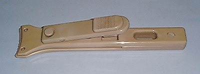
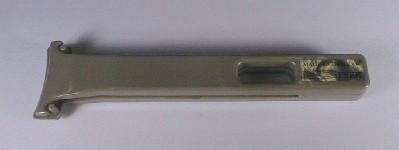
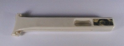
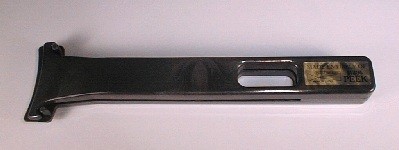
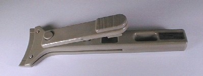
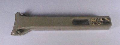
Teflon Tweezer

Teflon Tweezer

MSE SEMI 2012. 9. 12. 20:36

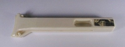
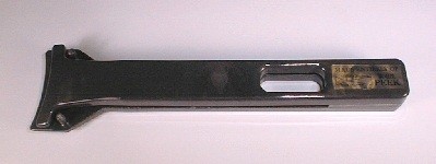
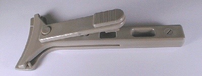
                                  TeflonTweezer                            


  • For substrate handling
  • Packaged in protective cases, additional cases available


C01

C14

C20


Part Number Tip Style and Size Overall Size Notes Material
C01-0315  * Rounded, 0.8mm (0.03") radius 127mm x 13mm
nominal Width
 Round Tip With 0.8mm Radius ETFE
C14-0315 Thin Tapered Tip 127mm Tips slightly heavier than C10 and C12 ETFE
C20-0215 Rounded, 1.5mm (0.06") radius 127mm x 13mm

Extra heavy for much stronger grip at ends PFA
C30-0215 Tip Wide  9.6mm 152mm
wide tip Offer More Holding Area For Safer handling At The Substrare Perimeter PFA
C50-0315 Tip Wide 19mm 254mm Squared off Tips Ideal For handling Large Plates ETFE
C52-0215 Tip wide 19mm 190mm Ideal For handling Large Plates PFA


           T- 11 Teflon Coated Tweezer                                              


  • "PTFE" Coated: These tweezers are made from chromosteel and then coated with "PTFE" (the whole tweezer). Suitable for electronic work and with conductive materials.

    arrow12Style #3C Very Fine Points, Short


    arrow12Style #5, Super Fine Points, Short

    Super Fine Points, Short Fontax Tweezers

    arrow12Style #7, Curved and Fine Po

    Curved and Fine Points Fontax Tweezers


  •                                                                                 


           C - 21                                                                               C-22 PTFE Forcep A:Sharp B:Square

           Poly Propylene Tweezer     


     POM Yellow & PMP White Tweezer

     POM Tweezer : 110도 내열 

     PMP Tweezer : 180도 내열


              T-23 Teflon Forcep(115mm)


           4-inch Semiconductor Wafer Handling

    • Designed to handle 4 inch semiconductor wafers
    • Withstand up to 130C continuously
    • No glue or metal parts
    M100-100
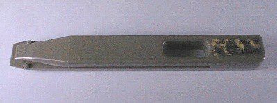
    PEEK Wafer Tweezers for 100mm (4-inch) Semiconductor Silicon Wafer Handling: Our unique design ensures to handle a delicate and fragile semiconductor wafer softly but firmly without excessive touch. ESD tweezers and vacuum pens for SMD/die handling are available.
    Made of PEEK 
    Wafer edge contact: 5.4mm(Top), 9.5mm(Bottom)
    Length: 146mm, Weight: 30g


    M110-100
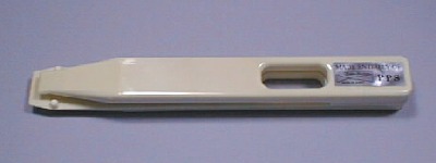
    PPS Wafer Tweezers for 100mm(4-inch) Semiconductor Silicon Wafer Processing: The area that contacts wafer surfaces is optically-polished to reduce surface particle counts. ESD safe tweezers and vacuum pencils for die/SMD handling are also available.
    Made of PPS
    Wafer edge contact: 5.4mm(Top), 9.5mm(Bottom)
    Length: 146mm, Weight: 31g

    E100-100
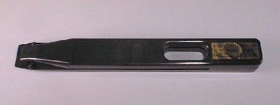
    Conductive PEEK Wafer Tweezers (ESD tweezers) for 100mm (4-inch) Semiconductor Silicon Wafer Process: The surfaces of a wafer are never scratched in contrast to conventional metal tweezers. ESD tweezers and vacuum pens for SMD/die handling are available.
    Made of Conductive PEEK
    Wafer edge contact: 5.4mm(Top), 9.5mm(Bottom)
    Length: 146mm, Weight: 30g


            5-inch Semiconductor Wafer Handling

    • Designed to handle 5 inch semiconductor wafers
    • Withstand up to 130C continuously
    • No glue or metal parts
    M100-125
    PEEK Wafer Tweezers for 125mm(5-inch) Semiconductor Silicon Wafer Process: The unique design ensures to handle a delicate and fragile semiconductor wafer softly but firmly without excessive touch. ESD tweezers and vacuum pencils for die/SMD handling are available.
    Made of PEEK
    Wafer edge contact: 4.5mm(Top), 9.0mm(Bottom)
    Length: 148mm, Weight: 31g


    M110-125
    PPS Wafer Tweezers for 125mm(5-inch) Semiconductor Silicon Wafer Processing: The surfaces of a wafer are never scratched in contrast to conventional metal tweezers. ESD safe tweezers and vacuum pens for SMD/die handling are also available.
    Made of PPS
    Wafer edge contact: 4.5mm(Top), 9.0mm(Bottom)
    Length: 148mm, Weight: 32g

    E100-125
    Conductive PEEK Wafer Tweezers for 125mm(5-inch) Semiconductor Silicon Wafer Handling: The area that contacts wafer surfaces is optically-polished to reduce surface particle counts. ESD tweezers and vacuum pencils for SMD/die handling are also available.
    Made of Conductive PEEK 
    Wafer edge contact: 4.5mm(Top), 9.0mm(Bottom)
    Length: 148mm, Weight: 32g


           6-inch Semiconductor Wafer Handling

    • Designed to handle 6 inch semiconductor wafers.
    • Withstand up to 130C continuously
    • No glue or metal parts
    M100-150L
    PEEK Manual Wand for 150mm (6-inch) Semiconductor Silicon Wafer Handling: The unique design ensures to handle a delicate and fragile semiconductor wafer softly but firmly without excessive touch. ESD tweezers and vacuum pens for SMD/die handling also available.
    Less force is required to handle wafers thanks to the lockable lever.
    Made of PEEK
    Wafer edge contact: 3.0mm(Top), 6.0mm(Bottom)
    Length: 185mm, Weight: 71g


    M100-150
    PEEK Manual Wafer Tweezers for 150mm(6-inch) Semiconductor Silicon Wafer Processing: The surfaces of a wafer are never scratched in contrast to conventional metal tweezers. ESD safe tweezers and vacuum pens for SMD/die handling are also available.
    Made of PEEK
    Wafer edge contact: 5.6mm(Top), 8.5mm(Bottom)
    Length: 147mm, Weight: 31g

    M110-150
    PPS Manual Wafer Tweezers for 150mm (6-inch) Semiconductor Silicon Wafer Processing: The area that contacts wafer surfaces is optically-polished to reduce surface particle counts. ESD tweezers and vacuum pencils for SMD/die handling are also available.
    Made of PPS
    Wafer edge contact: 5.6mm(Top), 8.5mm(Bottom)
    Length: 147mm, Weight: 33g

    E100-150
    L series Wafer Tweezer no metal contamination: Conductive PEEK ESD Tweezers (Manual Wafer Tweezers) for 150mm(6-inch) Semiconductor Silicon Wafer Handling. ESD safe tweezers and vacuum pens for die/SMD handling are also available.
    Made of Conductive PEEK
    Wafer edge contact: 5.6mm(Top), 8.5mm(Bottom)
    Length: 147mm, Weight: 32g


           8-inch Semiconductor Wafer Handling

    • Designed to handle 8 inch semiconductor wafers
    • Withstand up to 130C continuously
    • No glue or metal parts
    M100-200L
    PEEK Manual Wand for 200mm (8-inch) Semiconductor Silicon Wafer Handling: The area that contacts wafer surfaces is optically-polished to reduce surface particle counts. ESD tweezers and vacuum pencils for SMD/die handling are available.
    Less force is required to handle wafers thanks to the lockable lever.
    Made of PEEK
    Wafer edge contact: 3.0mm(Top), 10.0mm(Bottom)
    Length: 180mm, Weight: 72g


    M100-200
    PEEK Manual Wand for 200mm(8-inch) Semiconductor Silicon Wafer Process: The surfaces of a wafer are never scratched in contrast to conventional metal tweezers. ESD safe tweezers and vacuum pens for SMD/die handling are also available.
    Made of PEEK
    Wafer edge contact: 8.0mm(Top), 11.9mm(Bottom)
    Length: 147mm, Weight: 32g

    M110-200
    PPS Manual Wand for 200mm (8-inch) Semiconductor Silicon Wafer Process: Our unique design ensures to handle a delicate and fragile semiconductor wafer softly but firmly without excessive touch. ESD tweezers and vacuum pens for die/SMD handling are available.
    Made of PPS
    Wafer edge contact: 8.0mm(Top), 11.9mm(Bottom)
    Length: 147mm, Weight: 33g

    E100-200
    Conductive PEEK Manual Wand (ESD Tweezers) for 200mm(8-inch) Semiconductor Silicon Wafer Processing: Withstands up to 130C continuously. ESD safe tweezers and vacuum pens for SMD/die handling are also available.
    Made of Conductive PEEK
    Wafer edge contact: 8.0mm(Top), 11.9mm(Bottom)
    Length: 147mm, Weight: 33g


          12-inch Semiconductor Wafer Handling

    • Designed to handle 12-inch semiconductor wafers
    • Withstands up to 130C continuously
    • No glue or metal parts
    M100-300L
    PEEK Wafer Tweezers for 300mm(12-inch) Semiconductor Silicon Wafer Process: The unique design ensures to handle a delicate and fragile semiconductor wafer softly but firmly without excessive touch. The surfaces of a wafer are never scratched in contrast to metal tweezers. Vacuum pens for SMD/die handling are available.

    .

    Made of PEEK
    Wafer edge contact: 10mm(Top), 16mm(Bottom)
    Length: 180mm, Weight: 77g


      제품에 대한 문의사항이 있으시면 아래 e-mail, 전화 문의 바랍니다.

    MSE : 02-2275-9510     팩스 : 02-2278-5446 

    msescy@hanmail.net   http://semims.com