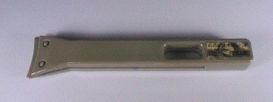
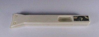
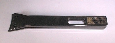
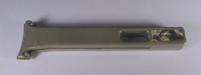
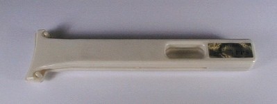
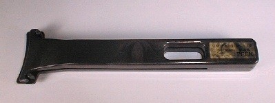
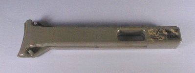
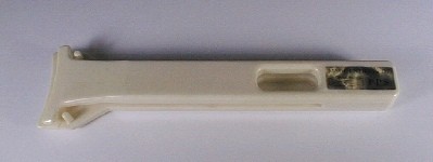
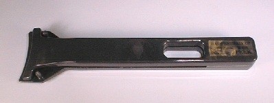
4" Wafer Tweezer 6-8" Wafer Tweezer


|
4-inch Semiconductor Wafer Handling
- Designed to handle 4 inch semiconductor wafers
- Withstand up to 130C continuously
- No glue or metal parts
|
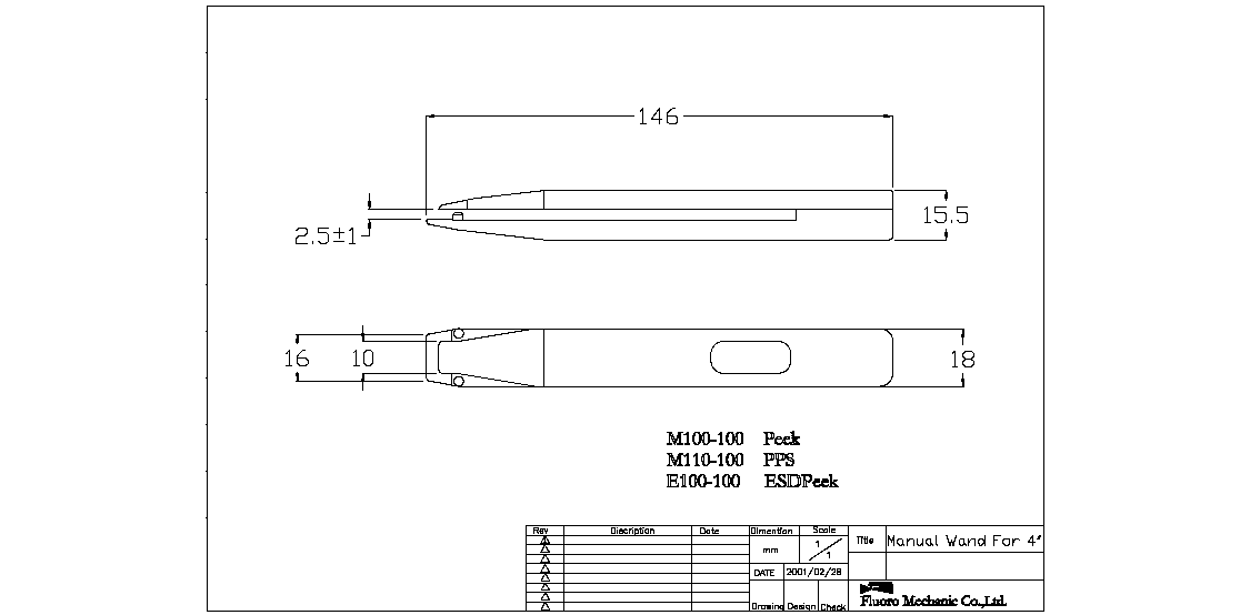
| M100-100 |
 |
| Made of PEEK |
| Wafer edge contact: 5.4mm(Top), 9.5mm(Bottom) |
| Length: 146mm, Weight: 30g |
| M110-100 |
 |
| Made of PPS |
| Wafer edge contact: 5.4mm(Top), 9.5mm(Bottom) |
| Length: 146mm, Weight: 31g |
| E100-100 |
 |
| Made of Conductive PEEK |
| Wafer edge contact: 5.4mm(Top), 9.5mm(Bottom) |
| Length: 146mm, Weight: 30g |
5-inch Semiconductor Wafer Handling
- Designed to handle 5 inch semiconductor wafers
- Withstand up to 130C continuously
- No glue or metal parts
|
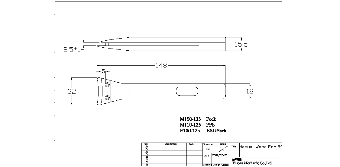
| M100-125 |
 |
| Made of PEEK |
| Wafer edge contact: 4.5mm(Top), 9.0mm(Bottom) |
| Length: 148mm, Weight: 31g |
| M110-125 |
 |
| Made of PPS |
| Wafer edge contact: 4.5mm(Top), 9.0mm(Bottom) |
| Length: 148mm, Weight: 32g |
| E100-125 |
 |
| Made of Conductive PEEK |
| Wafer edge contact: 4.5mm(Top), 9.0mm(Bottom) |
| Length: 148mm, Weight: 32g |
6-inch Semiconductor Wafer Handling
- Designed to handle 6 inch semiconductor wafers.
- Withstand up to 130C continuously
- No glue or metal parts
|
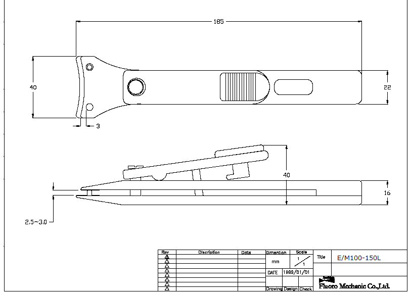
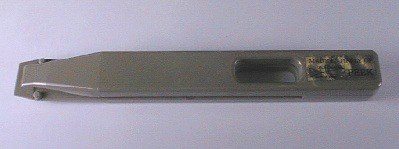
| M100-150L |
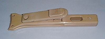 |
| Less force is required to handle wafers thanks to the lockable lever. |
| Made of PEEK |
| Wafer edge contact: 3.0mm(Top), 6.0mm(Bottom) |
| Length: 185mm, Weight: 71g |
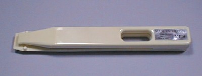
| M100-150 |
 |
| Made of PEEK |
| Wafer edge contact: 5.6mm(Top), 8.5mm(Bottom) |
| Length: 147mm, Weight: 31g |
| M110-150 |
 |
| Made of PPS |
| Wafer edge contact: 5.6mm(Top), 8.5mm(Bottom) |
| Length: 147mm, Weight: 33g |
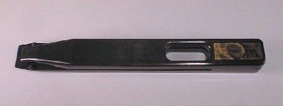
| E100-150 |
 |
| Made of Conductive PEEK |
| Wafer edge contact: 5.6mm(Top), 8.5mm(Bottom) |
| Length: 147mm, Weight: 32g | |
|
8-inch Semiconductor Wafer Handling
- Designed to handle 8 inch semiconductor wafers
- Withstand up to 130C continuously
- No glue or metal parts
|
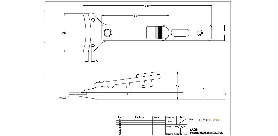
| M100-200L |
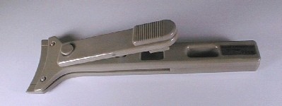 |
| Less force is required to handle wafers thanks to the lockable lever. |
| Made of PEEK |
| Wafer edge contact: 3.0mm(Top), 10.0mm(Bottom) |
| Length: 180mm, Weight: 72g |
| M100-200 |
 |
| Made of PEEK |
| Wafer edge contact: 8.0mm(Top), 11.9mm(Bottom) |
| Length: 147mm, Weight: 32g |
| M110-200 |
 |
| Made of PPS |
| Wafer edge contact: 8.0mm(Top), 11.9mm(Bottom) |
| Length: 147mm, Weight: 33g |
| E100-200 |
 |
| Made of Conductive PEEK |
| Wafer edge contact: 8.0mm(Top), 11.9mm(Bottom) |
| Length: 147mm, Weight: 33g |
12-inch Semiconductor Wafer Handling
- Designed to handle 12-inch semiconductor wafers
- Withstands up to 130C continuously
- No glue or metal parts
|
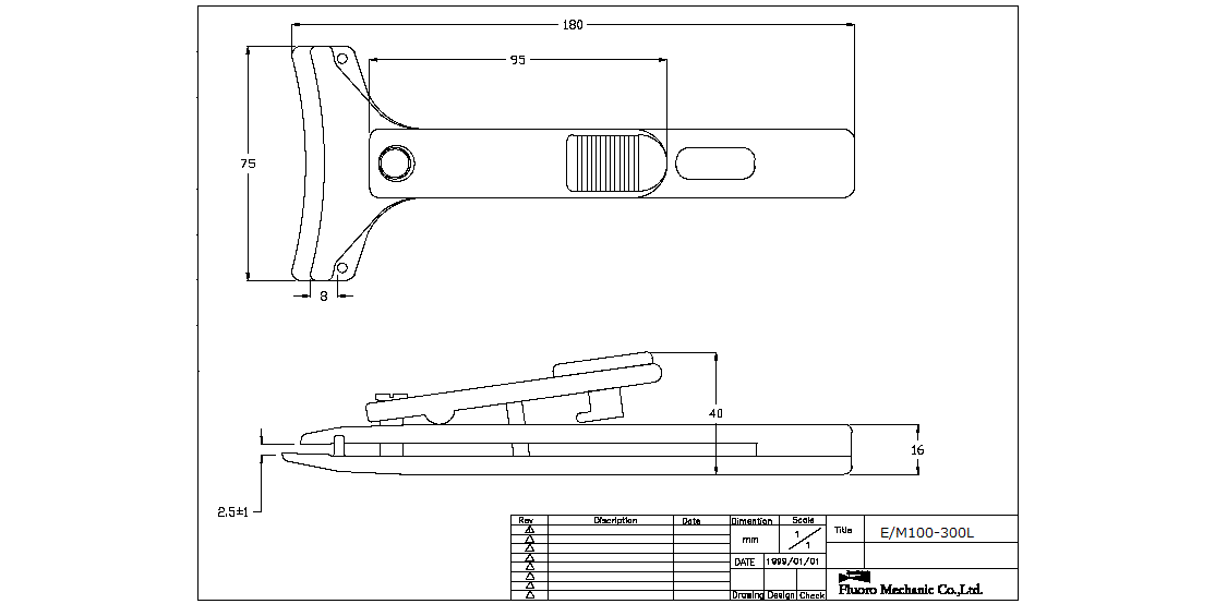
| M100-300L |
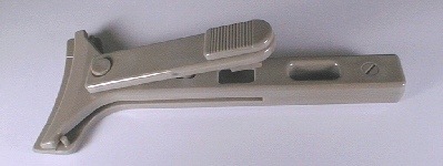 |
| Less force is required to handle wafers thanks to the lockable lever. |
| Made of PEEK |
| Wafer edge contact: 10mm(Top), 16mm(Bottom) |
| Length: 180mm, Weight: 77g |
|
제품에 대한 문의사항이 있으시면 아래 e-mail, 전화 문의 바랍니다.
| |